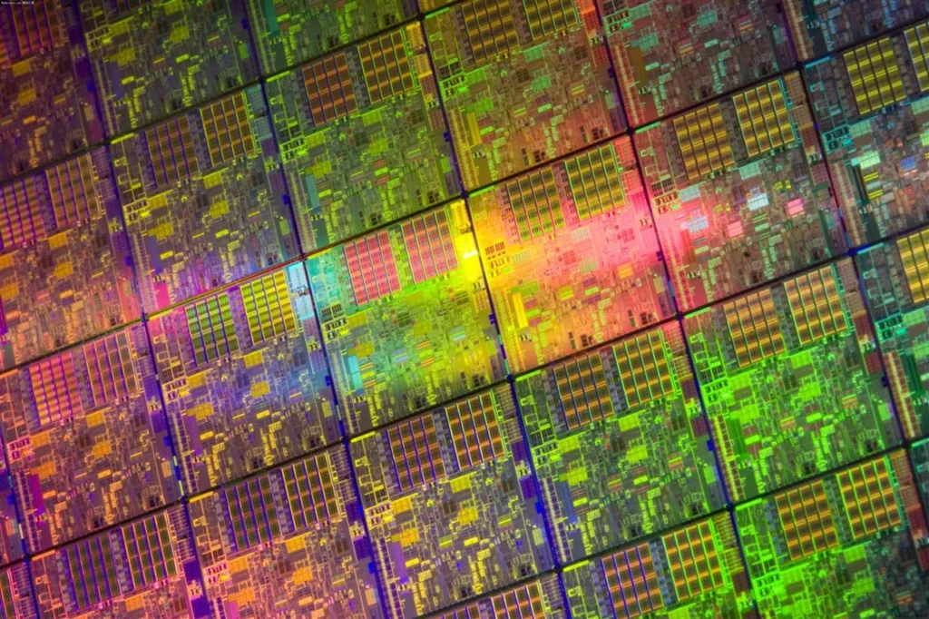
A wafer is a thin, round silicon slice (similar to the "pizza crust") and serves as the "raw material substrate" for chip manufacturing. It is made from high-purity single-crystal silicon.
A chip (or die) is an individual circuit unit processed on a wafer through a series of complex steps (similar to "pizza slices"). Each chip contains a complete set of electronic components (transistors, resistors, etc.) and, once cut and packaged, becomes a processor, memory, or other electronic device component.
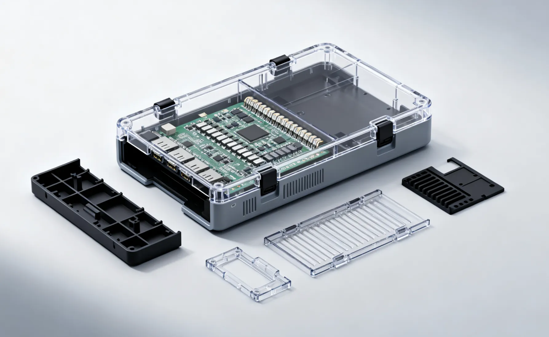
Chip packaging is a crucial step in semiconductor manufacturing. It involves cutting and separating the chip (die) from the wafer, then enclosing it in a protective shell using specific processes. The pad on the die is then connected electrically to the substrate and PCB.
Wafer and magnified grains under microscope:

Ensure stable operation of the chip in complex environments while providing an interface for signal transmission to external systems.
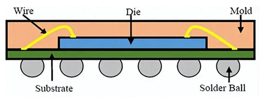
Basic Structure:
- Chip (Die): The core functional unit, cut from the wafer, containing the integrated circuit.
- Packaging Substrate: Supports the chip and provides electrical connections (e.g., wire bonding, flip-chip bonding).
- Wire: Creates the electrical connection between the chip and the packaging substrate.
- Encapsulation Material (Mold): Typically epoxy resin or ceramics that protect the chip from physical and chemical damage.
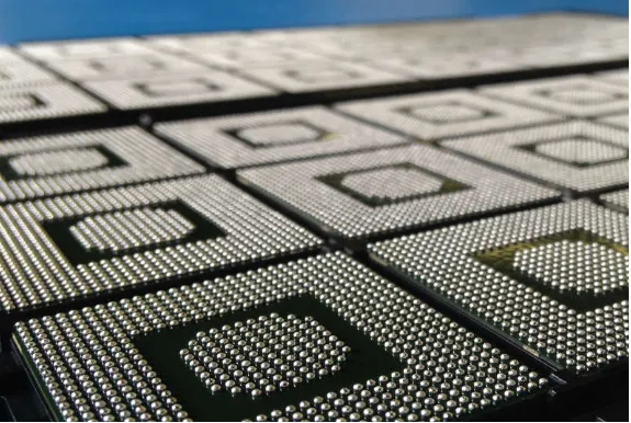
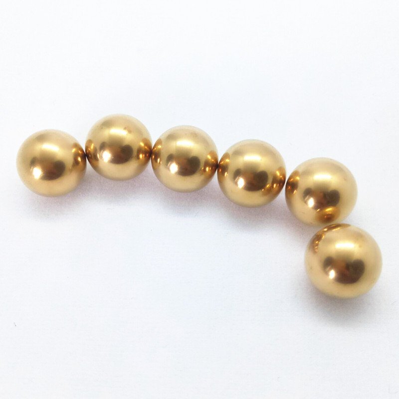
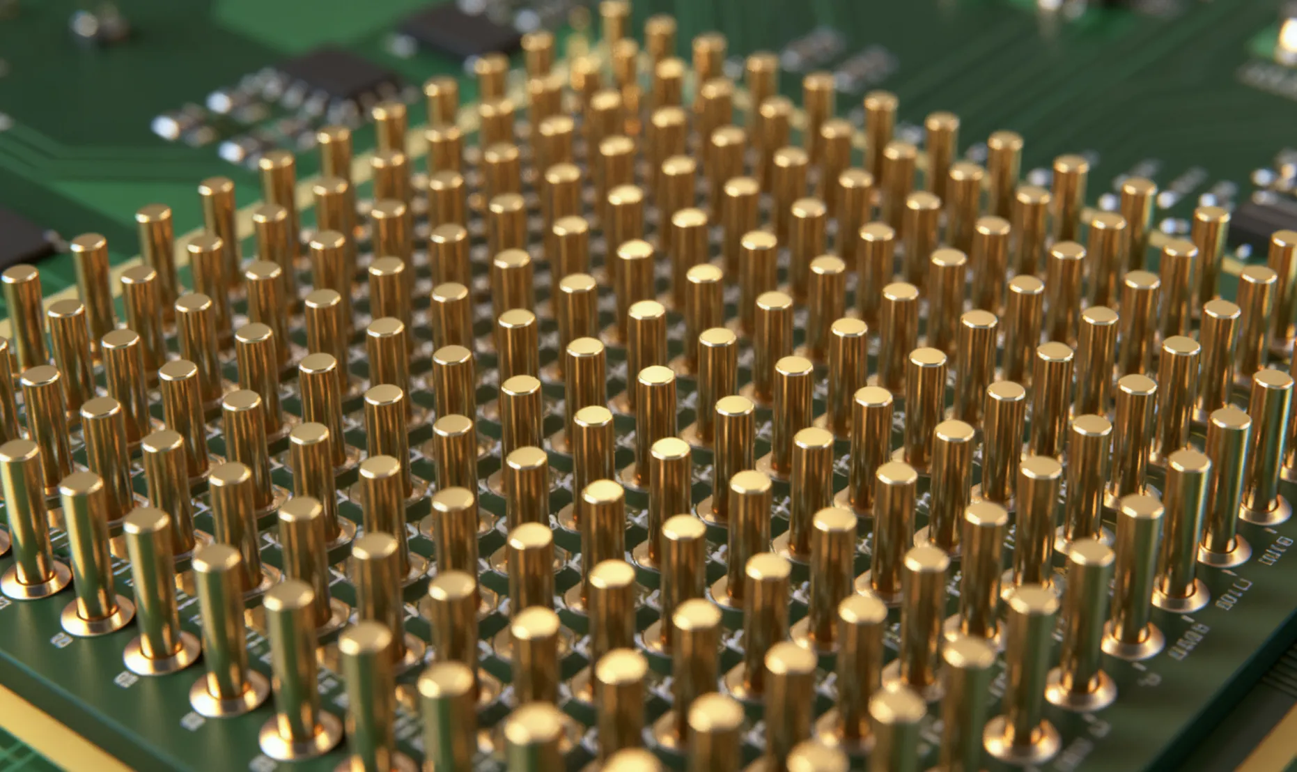
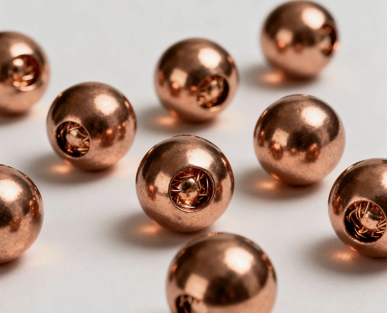
- Pins/Solder Balls: For example, solder balls in BGA (Ball Grid Array) packages connect the chip to the PCB.